

Why Semiconductor FABs are ditching the old ovens for IR curing
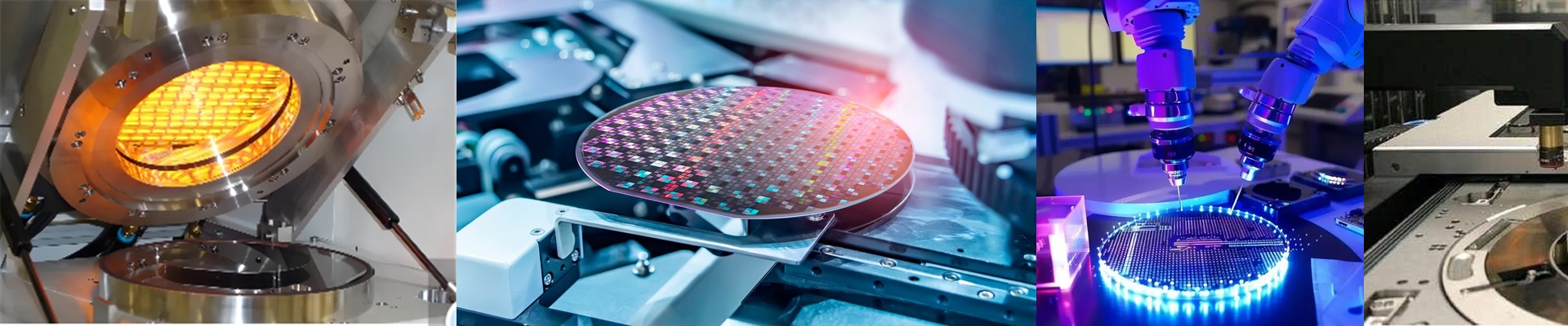
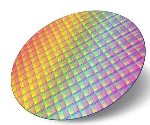
For a long time, semiconductor plants relied on big convection ovens and a lot of nasty chemicals to get the job done. But things are changing. More and more FABs are making the jump to infrared (IR) curing lamps. Why? Because they’re faster, cleaner, and they actually fit the push to go lead-free and eco-friendly. Stop heating the air Think about how a traditional oven works. You heat up the air, and then the air heats the wafer. It’s slow. It’s a waste of energy. IR is different. It’s direct. The lamps send out radiation that hits the photoresist or solder paste exactly where it needs to go. We use short-wave and medium-wave IR to punch through the surface layer instantly. Because it’s so efficient, we don’t have to lean on those VOC-heavy solvents or lead-based fluxes just to get the melting point down. Speed and the “Heat Problem” Lead-free alloys are picky. They need a steep temperature ramp to set correctly. To handle that, we use lamps with high wattage per linear inch. It’s fast. Really fast. We’re talking seconds instead of minutes. Plus, your equipment takes up way less room on the cleanroom floor. But there is a catch. When you’re pumping out that much energy, things get hot—fast. You have to make sure your exhaust systems are up to the task. If you don’t pull that waste heat away from the edges of the wafer, you’re looking at warping, and that’s a nightmare nobody wants. Keeping it clean The best part? IR systems are just… clean. You don’t have combustion by-products or weird air streams to filter. You aren’t blowing hot air all over a sterile environment, which means way fewer particles landing where they shouldn’t. And when a lamp finally gives out? It’s a breeze. You just pop the tube out, slide a new one in, check the connectors for any crusty oxidation, and you’re back in business. No complex chemical scrubbing systems, no headaches. Just a simple swap and you’re moving again.